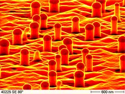
Silicon nanowires grown by molecular beam epitaxy
(based on) Schubert, Werner, Gösele et al
Appl. Phys. Lett. 84, 357 (2004)
Forschung » Halbleitende Nanodrähte

Halbleitende Nanodrähte
Zusammenfassung
This project deals with the controlled growth, the characterization, the
properties and potential applications of semiconductor nanowires and
nanocrystals in areas such as electronics, photonics, sensorics, and
photovoltaics for alternative energy generation. Depending on the size
of the structures quantum effects become an essential tool to tailor
the desired electronic properties.
Semiconductor materials form the basis of modern micro- and nano-electronic
chip, optoelectronics devices and many sensors. Life in a modern society
without electronic chips in computers, mobile phones, and cars is hardly
imaginable. Continuing device shrinking as expressed in Moores law is
accomplished by a top-down approach involving lithographic techniques.
A potential limit of this scaling approach might occur in the range of
about ten nanometers or even below.
All major semiconductor companies work on alternatives beyond this limit.
In the last five years the major contenders for potential structures
beyond normal microelectronics have turned out to be carbon nanotubes
and semiconductor nanowires. The area of semiconductor nanowires for
nanoelectronic devices has especially been pushed by US research groups,
e.g. by the group of Charles Lieber at Harvard University. In Europe,
it was only recently noticed that this is a scientifically and
technologically critically important area. Based on the experience
of early work on silicon quantum wires by one of the principal
investigators the DFG Priority Program 1165, Nanowires and Nanotubes
was initiated by Dr. Margit Zacharias.
The growth of semiconductor nanowires can be accomplished by a number
of different methods, such as chemical vapor deposition (Christiansen).
The vapor-liquid-solid method, as originally developed about forty years
ago and appropriately modified in recent years, allows the growth of nanowires
with diameters down to a few nanometers.
Landesgeförderte Projekte
(Förderung 07/2005-06/2008)
